Materials similar to graphene for use in quantum cryptography
 Source: Fotolia
Single atomic layer semiconductor structures may find applications in quantum computing and quantum cryptography. Physicists, including Polish scientists, have discovered their new, unique properties. These structures (like graphene from graphite) are separated from another layer material: tungsten diselenide.
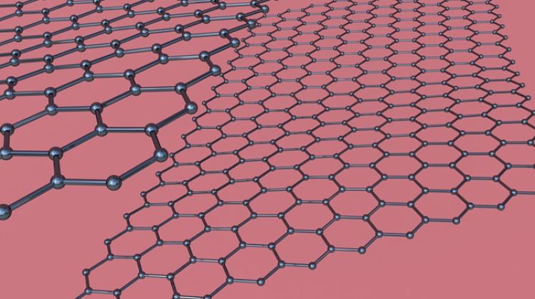
A single, atom-thick layer of material may have different properties than a multilayer crystal - this has been known for some time. Andre Geim and Konstantin Novoselov confirmed it undoubtedly for a single layer of carbon (graphene) obtained from graphite. Also for this, these researchers received the Nobel Prize in 2010.
"Everyone was immediately amazed with graphene. But there were attempts to separate individual layers of other materials. Among them is a class of materials, on which we focus in our research. They are the so-called dichalkogenides of transition metals" - said one of the study authors, Marek Potemski, who leads the group "Semiconductors and Nano-physics" in the French High Magnetic Fields Laboratory CNRS. He clarified that among the materials that raise high hopes are semiconductor compounds such as tungsten and molybdenum disulfides and diselenides. In particular, their specific electron properties inspire alternative direction in spintronics, known as valleytronics.
One of the authors of the study, Maciej Koperski from the University of Grenoble and the Faculty of Physics, University of Warsaw, commented: "People are trying to find alternatives for electronics, which is based on binary logic circuits, the zero-ones. In a large simplification, future solutions, such as spintronics, could use the entire spectrum of values between zero and one, and you could think the same about valleytronics with regard to the materials covered by our research". He admitted that the applications of sources of single photons may in the future include data storage using light and data transmission in a way inaccessible to intruders.
In this latest study - published in "Nature Natotechnology" - physicists, including Polish scientists, showed new unique characteristics of thin films of tungsten diselenide. Moreover, their findings are consistent with the results of the three other projects, published in the same issue of "Nature Nanotechnology". All four consistently show that these layers thanks to their particular characteristics, can be used, for example, in quantum cryptography or in the work on quantum computer.
Tungsten diselenide is a crystal that looks a bit like graphite. "Similarly to isolating graphene, you need to work hard to separate a single layer of high-quality from a piece of tungsten diselenide" - admitted Marek Potemski. However, previous studies have shown that it is worth it. It is well know that a single layer of semiconductor dichalkogenides takes on the characteristics of a semiconductor with a simple energy gap, and that means it readily emits light.
Physicists (in addition to Marek Potemski and Maciej Koperski, Piotr Kossacki from the Faculty of Physics, University of Warsaw participated in research) showed, however, that the process of emitting light at the edges of tungsten diselenide cuts can occur in a particular way - at the same moment, just one photon is emitted, not many photons simultaneously. "These light sources are a sought after element in quantum computing, in particular in cryptography" - said Marek Potemski and explained that in quantum computing operations are performed on single photons.
Sources of single photons associated with tungsten diselenide join now to the class of other such sources, such as single molecules, some defects in diamonds, quantum dots, nanocrystals. "Many such objects are known, but we expect that our single-photon emitters have specific properties inherited from atomic thickness layers" - said Koperski.
Identification of sources of single photons in layers of tungsten diselenide opens up new possibilities for scientists. There is a strong interest in so-called trigger van der Waals heterostructures, superposed layers of atomic thickness, each layer composed of materials with different properties. Such a multilayer structure with elements in the form of various semiconductors, insulators, metals and semimetals would be a multifunction device. For example, one layer would act as a light source, another as a microwave source, yet another as a detector or sensor, and in the light of the most recent work, yet another as a source of single photons. Importantly, all of this together would have microscopic dimensions.
"In the world, and particularly in Europe work on graphene is already very advanced. It is expected that functioning device will be designed soon. In contrast, work on other layered materials - including our work - are in the phase of basic research" - noted Marek Potemski.
"Although more and more is known about the materials that would be useful in quantum computing and cryptography, we will probably have to wait many years for a useful quantum computer" - he added.
PAP - Science and Scholarship in Poland, Ludwika Tomala
lt/ mki/ mrt/
tr. RL
Przed dodaniem komentarza prosimy o zapoznanie z Regulaminem forum serwisu Nauka w Polsce.