Microlenses to View Nanoworld
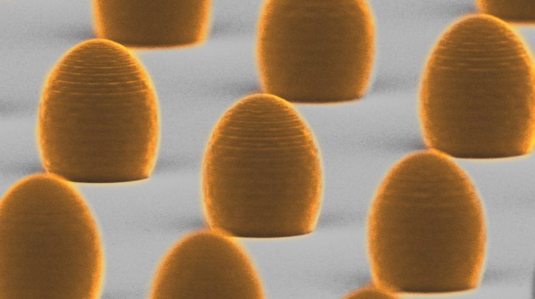 3D printed aspheric microlenses, electron microscope image. The diameter of each lens is 15 micrometres, or about one-fifth of the thickness of a human hair. Thanks to the high efficiency of 3D printing, it is possible to produce hundreds of microlenses on one substrate in a short time. (Credit: Faculty of Physics, University of Warsaw, A. Bogucki and Ł. Zinkiewicz)
Microscopic polymer lenses with dimensions many times smaller than the diameter of a human hair, make it possible to examine nano-objects without using a microscope.
Developed by scientists from the University of Warsaw in cooperation with foreign colleagues, the lenses were produced with ultra-precise 3D laser printing technology.
Already hailed as being the third industrial revolution, 3D printing technology, consists of layer-by-layer printing of a three-dimensional object based on a computer model.
According to the Faculty of Physics of the University of Warsaw: “These lenses increase the amount of light that can be observed from samples containing, for example, quantum dots or the recently extremely popular atom-thin two-dimensional materials.
“The latter include molybdenum diselenide and tungsten diselenide, which have a graphene-like structure. Printed microlens surface forms the light emitted from the sample into a beam of photons with low divergence, which can be easily sent to research and measuring equipment.
“This microlens can replace expensive and bulky microscope lens.”
Typical high-grade microscope lenses are approximately the size of a cucumber and weigh up to half a kilogram. They must be precisely placed at an appropriate distance (less than a few millimetres) from the sample.
This imposes significant restrictions on the performance of many experiments in the field of semiconductor physics, such as measurements in high (pulse) magnetic fields, at very low temperatures or with the use of microwave radiation. The lenses operate both at extremely low temperatures (close to absolute zero) and in huge magnetic fields that do not occur naturally on our planet.
The Faculty of Physics said: “3D printing is very efficient, so you can produce hundreds of microlenses on one substrate in a short time. Arranged in a regular network, like figures on the chessboard, they form a coordinate system on the sample.
“It makes it possible to accurately determine the location of the selected light emitter in a semiconductor sample. This in turn, allows for repeated measurements of the same emitter in various laboratories around the world. Until now, locating a given illuminating object in the sample again has been very time consuming.
“From the point of view of basic research, the possibility of returning to the same emitter is priceless, as it significantly increases the efficiency of measurements and facilitates testing of new hypotheses.”
A slight modification of the shape of the proposed microlenses allows them to produce them using large-scale industrial duplication methods, such as matrix imprinting. The next step for researchers will be to adapt the lens design to the requirements of fibre optic technology, which is the future of light-based devices.
PAP - Nauka w Polsce
ekr/ agt/ kap/
tr. RL
Przed dodaniem komentarza prosimy o zapoznanie z Regulaminem forum serwisu Nauka w Polsce.